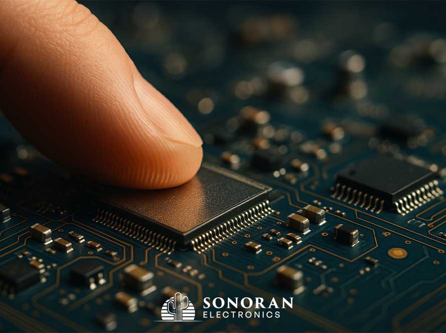
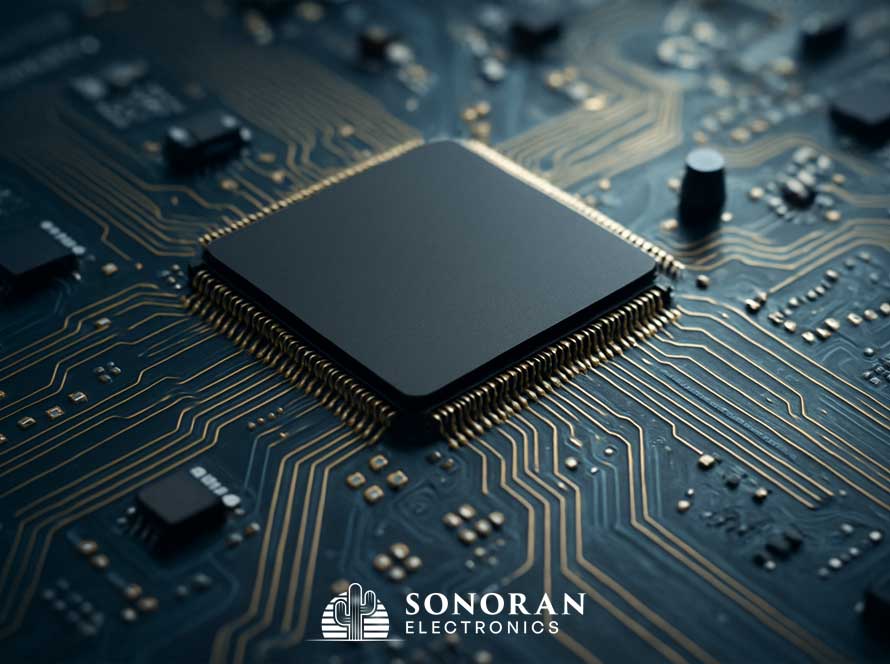
For decades, Moore’s Law—a prediction that the number of transistors on a microchip would double approximately every two years—has served as a guiding principle for the semiconductor industry. This observation has driven remarkable advancements in microelectronics, enabling faster, smaller, and more efficient devices. However, as transistors approach their physical limits, the industry faces a critical challenge: how to sustain progress when traditional scaling is no longer feasible.
The foundation of Moore’s Law lies in the continuous miniaturization of transistors. Yet, as these components shrink to dimensions measured in nanometers, several barriers emerge. Quantum tunneling, where electrons pass through thin insulating layers, undermines transistor performance. Heat dissipation becomes a major concern as tightly packed circuits generate excessive energy loss. Additionally, the cost of advanced fabrication processes has soared, making it increasingly difficult to maintain the pace of innovation.
These challenges suggest that the era of conventional semiconductor scaling is nearing its end. In response, the industry is exploring alternative paths to maintain progress.
One promising avenue is chiplet architecture, where multiple smaller chips are integrated into a single package. Instead of relying on monolithic designs, chiplets allow manufacturers to combine different functionalities on separate components, enhancing performance while controlling costs. This modular approach is already being adopted by leading companies to develop high-performance processors for data centers and AI applications.
Another breakthrough involves 3D integration, where chips are stacked vertically instead of spread out horizontally. By layering circuits, engineers can achieve higher density and improved performance without increasing the chip’s footprint. Advances in through-silicon vias (TSVs) and wafer bonding technologies are making this approach more viable, particularly for memory-intensive applications.
The reliance on silicon as the primary material for semiconductors is also being reexamined. Wide-bandgap materials like Gallium Nitride (GaN) and Silicon Carbide (SiC) offer superior performance in high-power and high-frequency applications. Meanwhile, graphene and other two-dimensional materials are being studied for their potential to enable ultra-fast and energy-efficient devices.
Another exciting development is the use of nanowires and nanosheets, which offer better electrostatic control over transistors compared to traditional designs. These structures are particularly promising for next-generation field-effect transistors (FETs), helping to push the boundaries of miniaturization.
In the quest to extend Moore’s Law, extreme ultraviolet (EUV) lithography has emerged as a critical technology. EUV enables the creation of smaller, more precise patterns on wafers, allowing for higher transistor densities. While EUV systems are expensive and complex, their adoption is growing, with leading foundries investing heavily to keep pace with demand.
Beyond EUV, researchers are exploring next-generation lithography techniques, such as nanoimprint lithography and directed self-assembly. These methods could offer cost-effective solutions for producing sub-nanometer features in future chips.
Artificial intelligence (AI) is not just a driver of demand for microelectronics—it is also transforming how chips are designed and manufactured. AI-powered tools can optimize layouts, predict failure points, and simulate performance under various conditions, accelerating development cycles. This integration of AI into semiconductor engineering represents a significant shift in how progress is achieved.
As the industry moves beyond traditional scaling, innovation is shifting toward enhancing functionality rather than just increasing transistor count. Concepts like heterogeneous integration, where chips with different technologies are combined, are gaining traction. Additionally, neuromorphic computing, which mimics the brain’s architecture, is being explored to improve efficiency for AI workloads.
The transition beyond Moore’s Law marks a turning point for microelectronics. While challenges remain, the industry is demonstrating remarkable resilience by embracing new architectures, materials, and technologies. Collaboration between academia, industry, and governments will be essential to overcoming barriers and unlocking the full potential of next-generation semiconductors.
In this new era, success will be defined not by how small transistors can become, but by how effectively technology can adapt to the demands of a rapidly evolving world. By rethinking the principles of chip design and manufacturing, the microelectronics industry is poised to continue its legacy of innovation, even in a post-Moore’s Law landscape.

