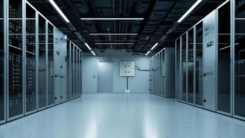
Artificial intelligence is transforming nearly every segment of the semiconductor industry, but perhaps nowhere is the impact more visible than in the memory market.
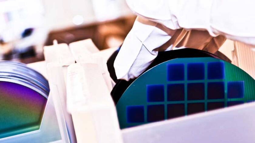
The global artificial intelligence boom has created unprecedented demand for advanced semiconductors, transforming Taiwan Semiconductor Manufacturing Company (TSMC) into one of the most strategically important companies in the world.
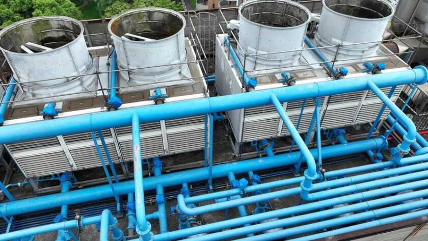
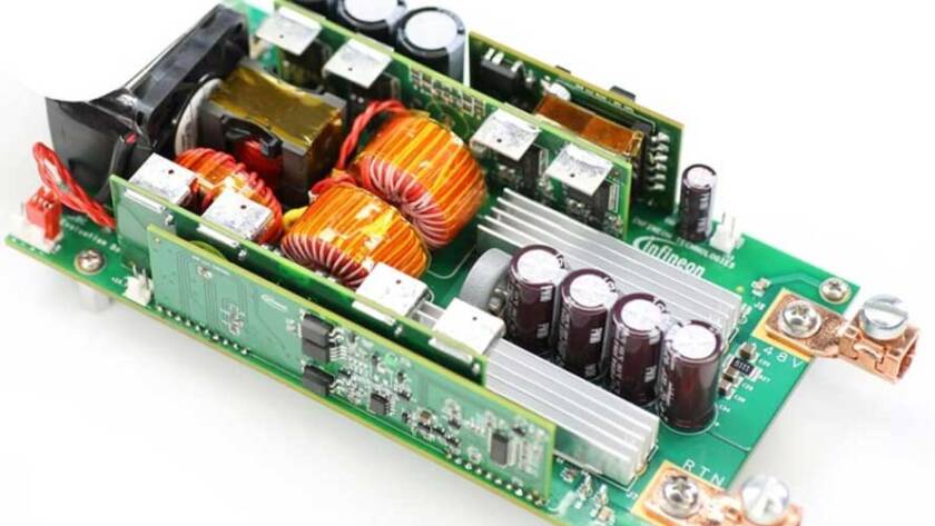
The expansion of AI infrastructure is typically framed in terms of compute and memory. That framing overlooks a constraint that is becoming increasingly difficult to manage: power.
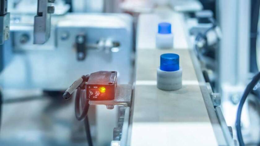
For much of the past two decades, supply chain strategy in the semiconductor and electronics industries was guided by a singular objective: efficiency.
The semiconductor industry has always experienced cycles of consolidation, often driven by cost pressures, scale requirements, and technological transitions.